Nishant BakshiAnalog / Mixed-Signal Design Engineer

Electrical engineer with an MSEE from USC (analog/mixed-signal IC design) and 2+ years in semiconductor reliability and test engineering. Background spans CMOS chip characterization, PCB design/bring-up, and audio hardware — currently designing loudspeaker systems and repairing vintage amplifiers at Common Wave Hi-Fi in Los Angeles.


Hardware Projects

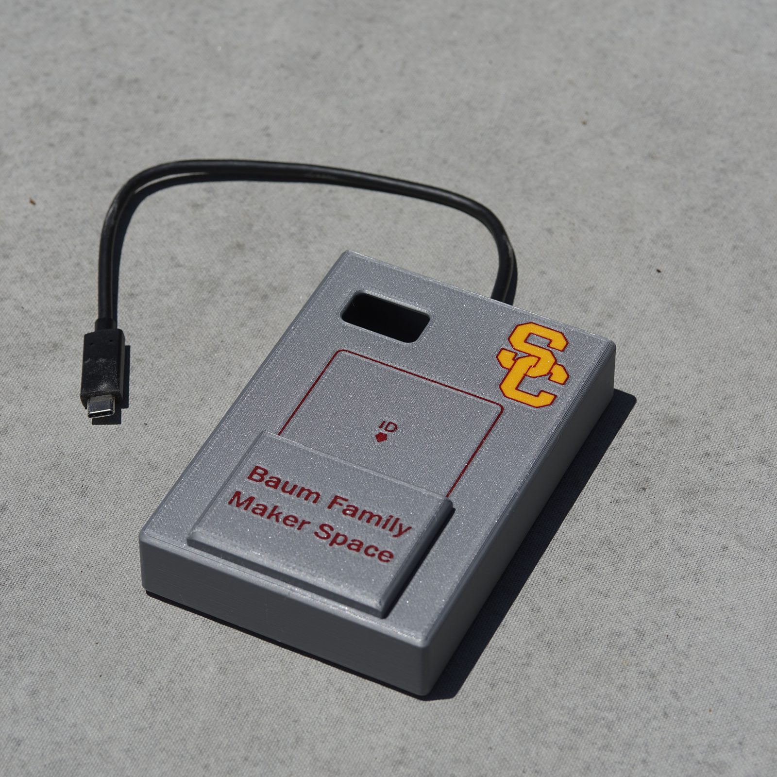
RFID Tool Lockout System

Work Project — USC Maker Space
aug 2025 – present

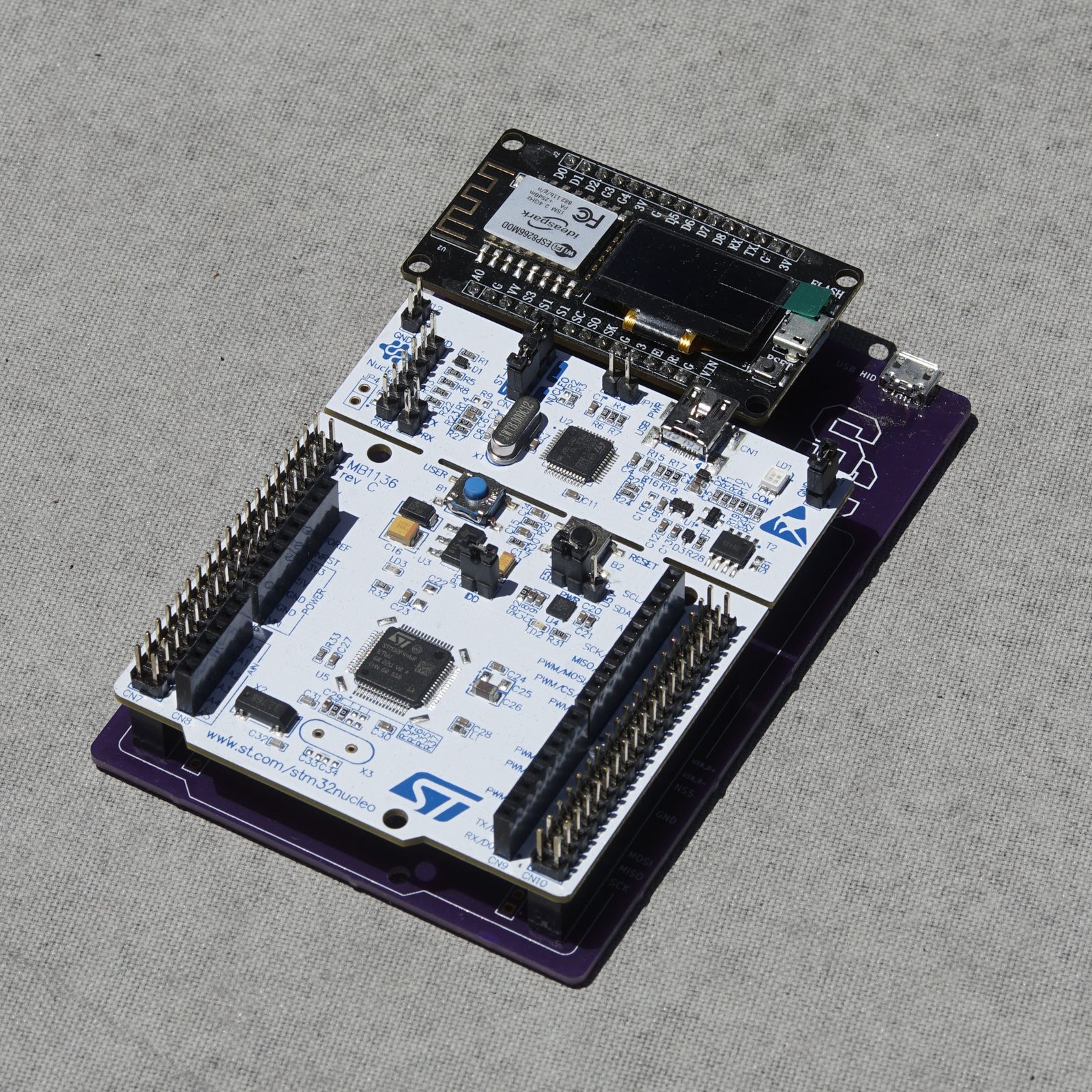
Access-control system for the Maker Space's laser cutters and waterjet, replacing shared passwords with university ID swipe access.

  • Replaced shared passwords and lockout codes with university ID swipe access on 2 laser cutters and 1 waterjet cutter
  • Developed ESP32 firmware in ESP-IDF (C/C++) for HID emulation and RFID UID reading
  • Designed a custom carrier PCB and 3D-printed enclosure for the dev board assembly
  • Building a cloud registration and staff-approval pipeline with wireless UID database sync to each device
  • Leading lab-wide rollout and designing a custom PN532 reader circuit to replace the dev board
S/H Test PCB — 64-Channel 640MHz Sample-and-Hold Chip

Research Project — IEDM Group, USC
may 2025 – may 2026

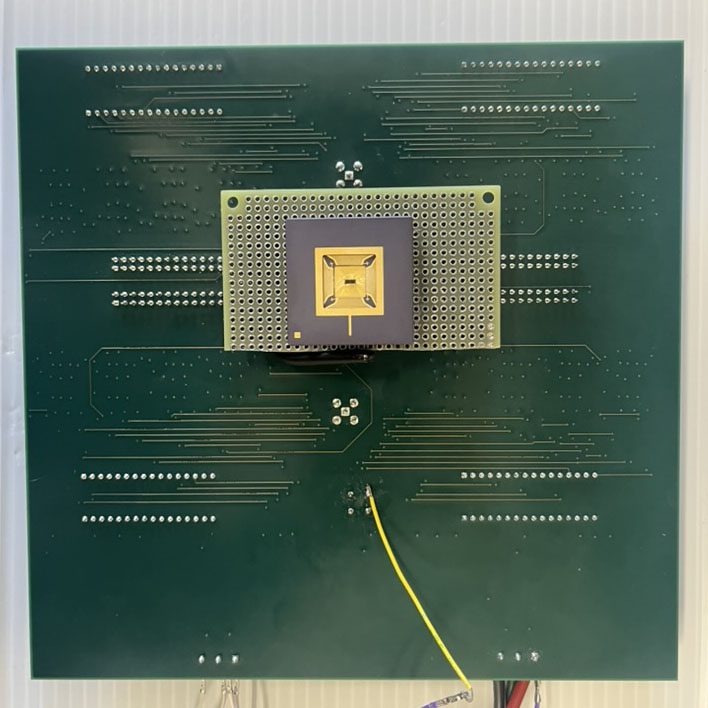
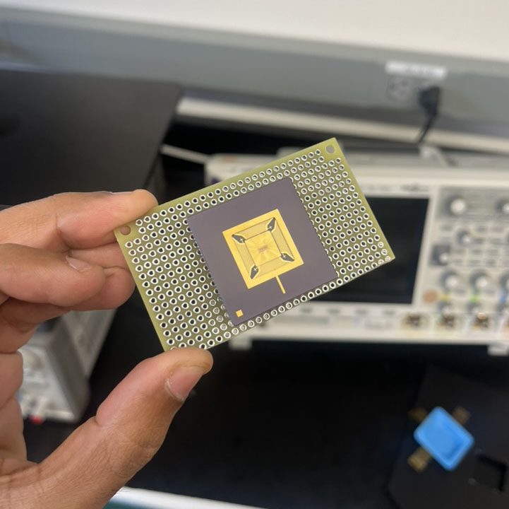
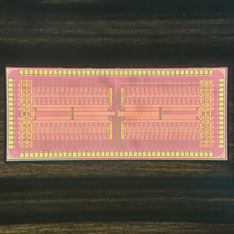
Test PCB design and bring-up support for a custom 64-channel, 640MHz sample-and-hold CMOS chip.

  • Designed a PGA-socketed test PCB and wirebonding diagram for the chip; interfaced with packaging vendors for assembly
  • Diagnosed and characterized the chip using probe stations, parametric analyzers, oscilloscopes, and an off-board ADC
  • Assembled, reworked, and brought up mixed-signal PCBs for chip validation, including SMD soldering and signal debugging
  • Contributed to a chip publication in IEEE Solid-State Circuits Letters ("A 1.2-V, 8.5-ns Settling, Bi-Slewing CMOS Driver for Heavy Loads in Discrete-Time Analog Computing Applications")

7W Class-A Power Amp

Personal Project
may 2025 – sep 2025

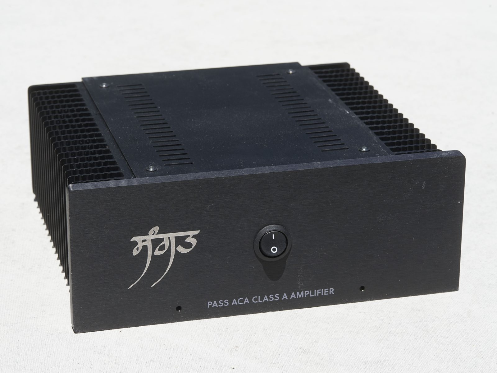
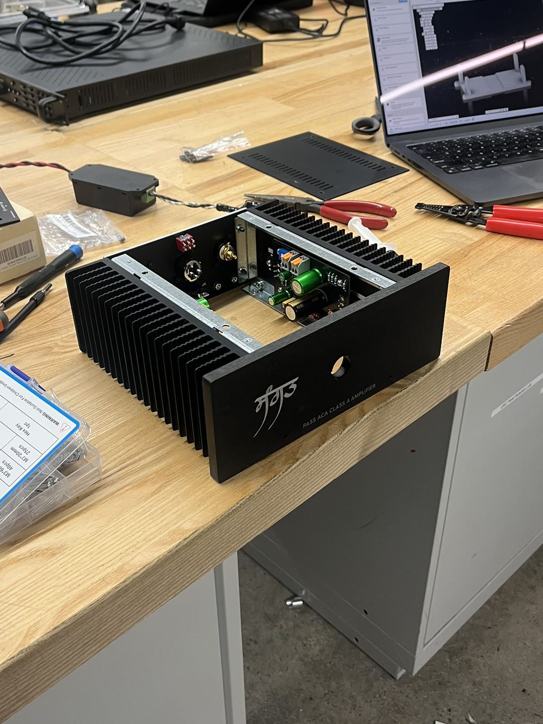
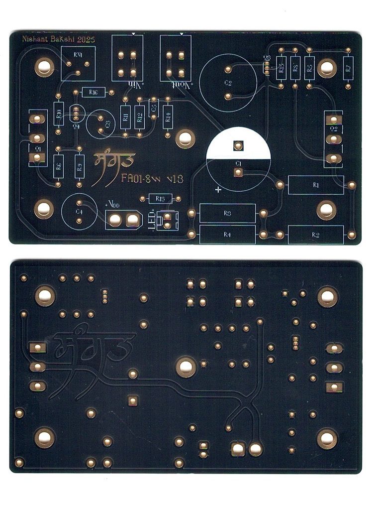
Single-ended Class-A amplifier built from schematic to finished chassis.

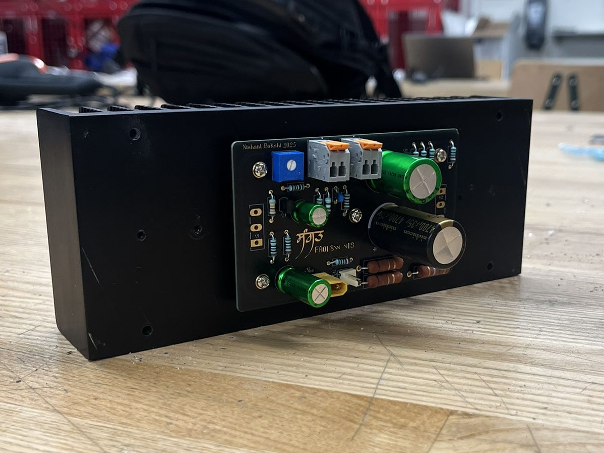
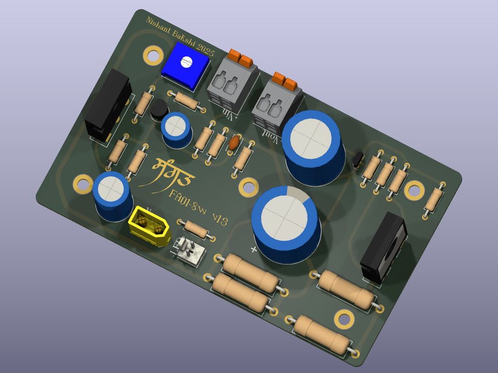
  • Designed a single-ended Class-A topology with NFET output, active load, JFET driver, and BJT current source
  • Laid out a through-hole PCB in KiCAD and hand-assembled the board
  • Integrated the amplifier into a heatsink-equipped chassis for thermal management of the Class-A bias current

Mini Onken Speaker

Personal Project
jan 2024 – may 2024

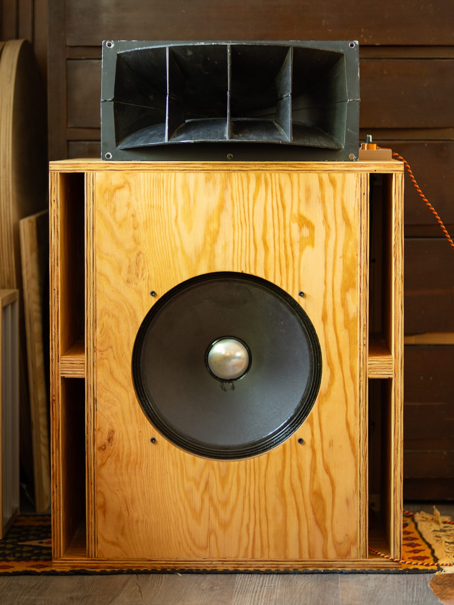
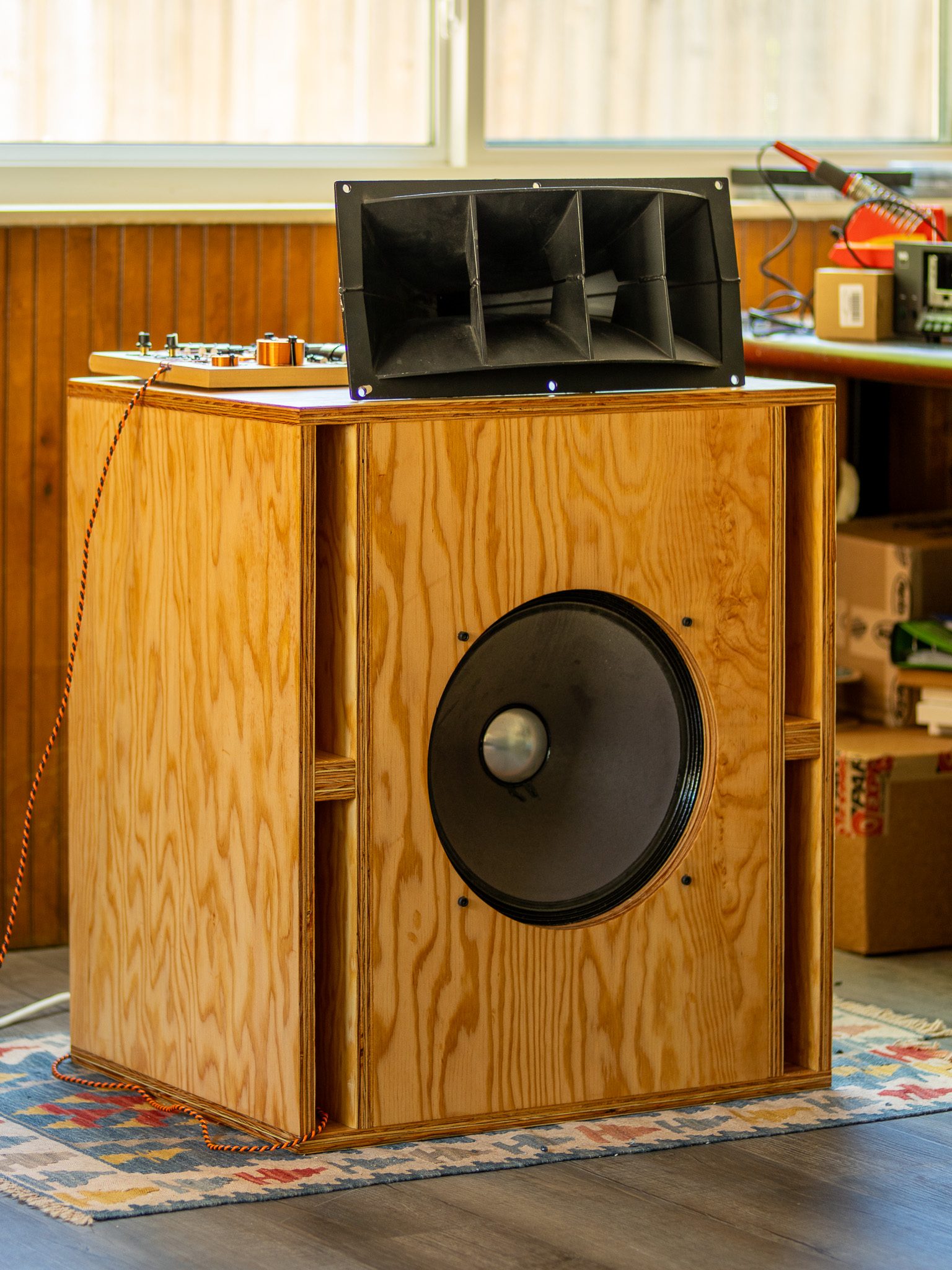
Scaled-down Onken enclosure built for vintage Altec drivers.

  • Designed an 8 cubic foot Onken enclosure with an external 811 sectoral horn for 1970s Altec drivers
  • Modeled the design using lumped-parameter simulation in VituixCAD and WinISD
  • Fabricated the cabinet from marine-grade Douglas fir plywood using Fusion 360 CAD/CAM and CNC routing
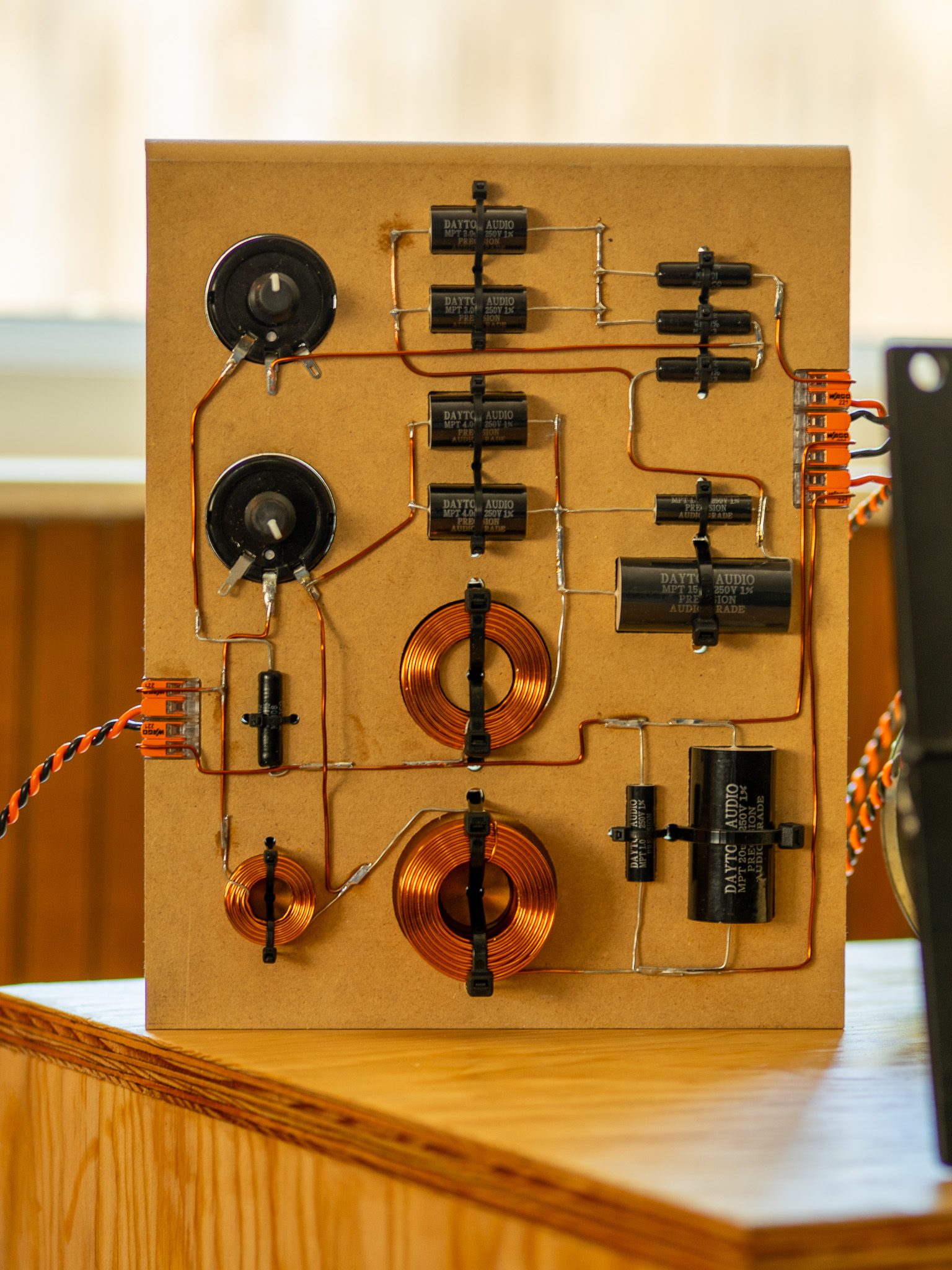
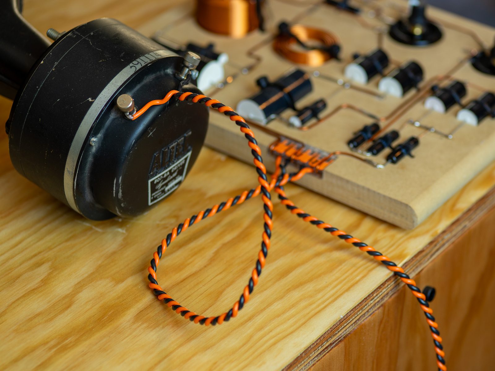
  • Designed, built, and bench-measured a crossover network based on the Altec Model 19 topology

Pocket Photometer

Volunteer Research — NYU MicroParticle Photo-Physics Lab
may 2021 – dec 2021

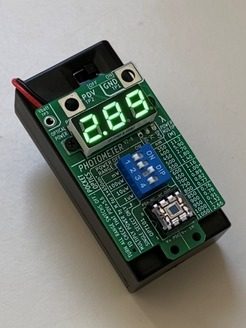
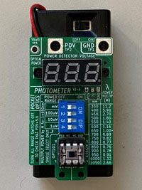
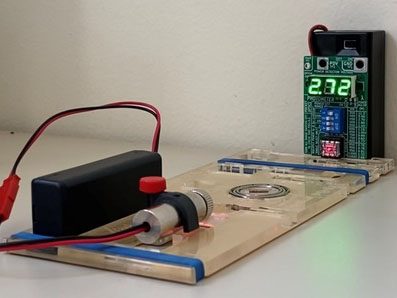
Battery-powered optical power meter for a take-home lab kit now sold commercially on Amazon.

  • Contributed to development of the Pocket Optics Kit (PO-1) optical power meter, now sold on Amazon
  • Simulated the TIA circuit in OrCAD Capture and laid out the PCB in KiCAD
  • Bench-tested the assembled board across 4 power ranges (1µW – 1mW) and a 350–1050nm wavelength range
  • Achieved 40–75% higher accuracy than smartphone light-meter apps

Circuit Design & Simulation

12-Bit 10MS/s Asynchronous SAR ADC

Class Project — EE631
mar 2025 – may 2025

12-bit, 10MS/s asynchronous SAR ADC designed in TSMC 45nm CMOS.

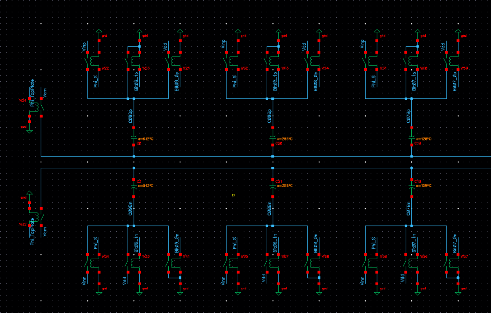
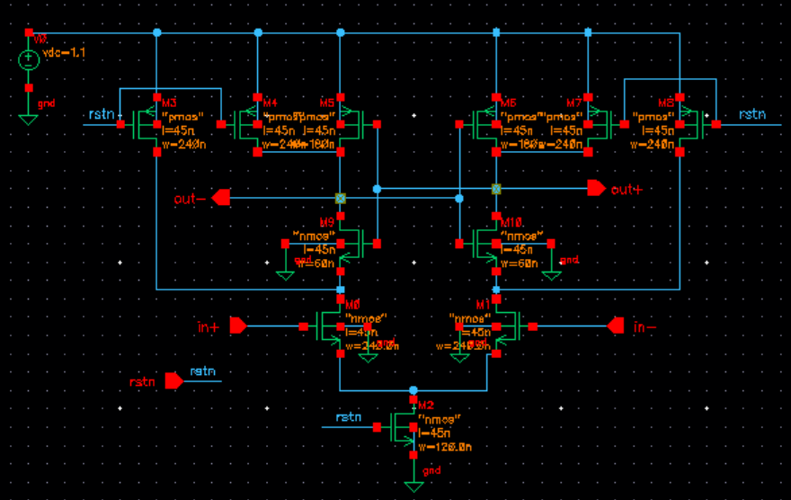
  • Designed the differential CDAC, strongarm comparator, D-flip-flops, and self-timed asynchronous control logic
  • Implemented monotonic switching and bottom-plate sampling to reduce pedestal error and eliminate static power
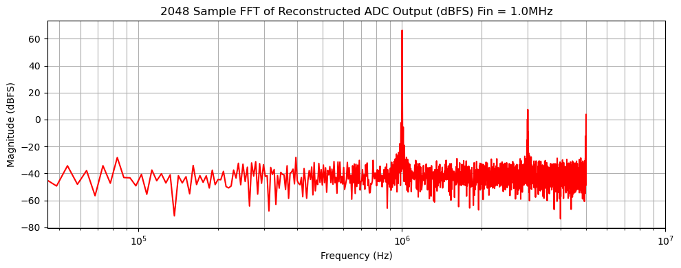
  • Simulated in Cadence Spectre with waveforms recovered via a custom Python script; achieved 9.03-bit ENOB (56.1 dB SNDR) at 1MHz
  • Developed a SPICE-netlist prompting method for AI-assisted transistor sizing (ChatGPT o3), producing one of the few functional AI-sized designs among 15 class teams

180nm 5.7GHz Rail-to-Rail OTA

Class Project — EE536A
oct 2024 – dec 2024

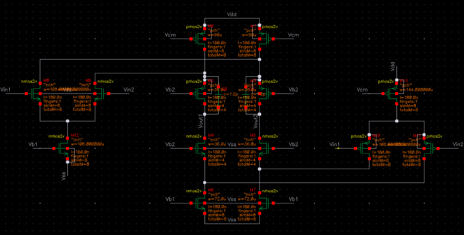
180nm CMOS rail-to-rail folded cascode OTA.

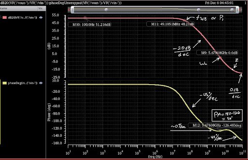
  • Achieved 51 dB DC gain, 5.7 GHz unity-gain bandwidth, and 0.77 nV/√Hz input-referred noise
  • Designed a Differential-Difference Amplifier (DDA) based common-mode feedback circuit adapted from IEEE literature, avoiding poly resistors for output common-mode setting
  • Standardized device sizing in practical multiples (e.g., 18µm increments) to align with Process Control Monitoring structures used in wafer-level characterization

250W 2-Switch Forward Converter

Class Project — EE528
mar 2026 – may 2026

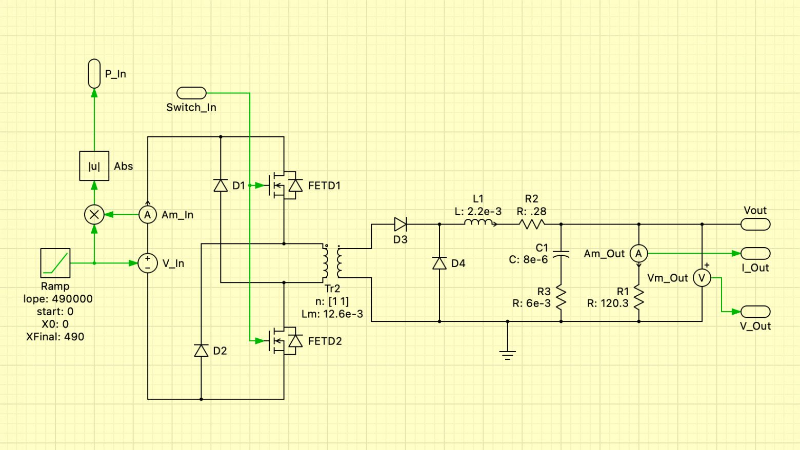
250W two-switch forward converter for medium-voltage DC-DC conversion.

  • Designed a 250W, 450VDC-to-190VDC converter with custom transformer and inductor magnetics
  • Selected Wolfspeed SiC MOSFETs and Schottky diodes for medium-voltage switching
  • Designed a Type-II compensator and feedback network for output regulation
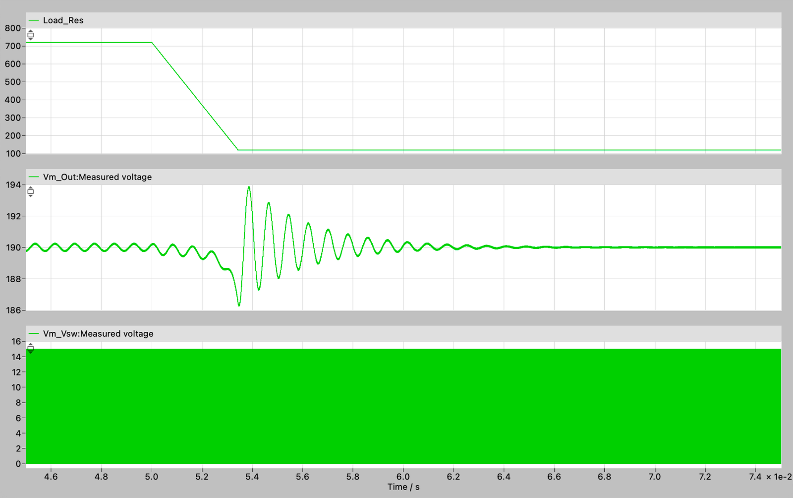
  • Simulated power stage and control loop performance in PLECS, achieving 92.6% efficiency at 300W with sub-2% output ripple during load transients